Service Details
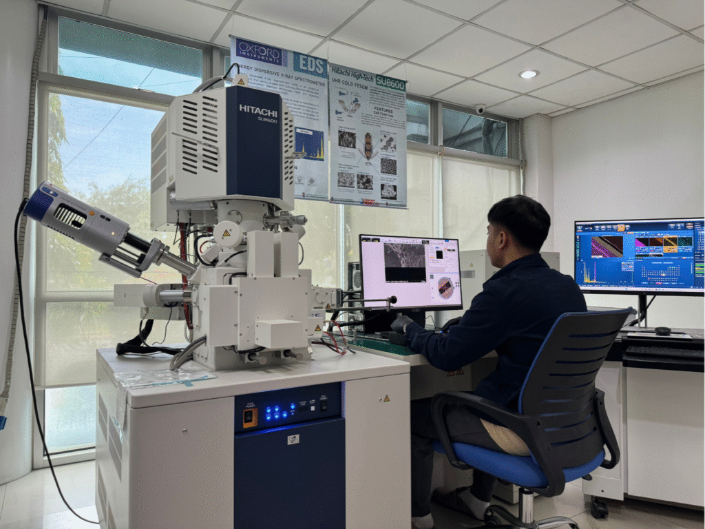
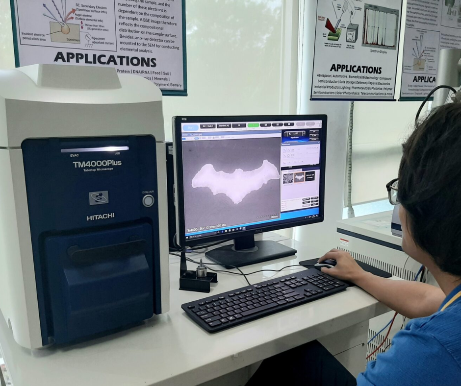
Scanning Electron Microscopy / SEM Imaging is a high-magnification imaging technique used to examine the surface morphology, texture, and microstructure of materials. It uses a focused electron beam to produce detailed images of samples at micro- to nanoscale levels. SEM is commonly used for failure analysis, material characterization, quality control, research and development, and inspection of metals, polymers, ceramics, semiconductors, coatings, particles, and other solid materials.
To support materials engineering, research, nanotechnology, and failure analysis, NASAT Labs is equipped with five different SEMs, including a cold field emission SEM (FE-SEM) capable of ultra-high resolution imaging down to 0.6 nm. Paired with advanced technologies like EDS and EBSD, our SEM systems deliver cutting-edge performance for surface and elemental analysis. With top-tier instrumentation and regularly trained staff, we ensure precision, reliability, and excellence in every analysis.
Common Applications
- Materials Science – Surface morphology, texture, defects, and microstructure analysis
- Failure Analysis – Crack, fracture, corrosion, contamination, and defect investigation
- Semiconductors & Electronics – Inspection of components, surfaces, patterns, and process-related defects
- Metals, Ceramics & Polymers – Evaluation of surface features, particles, grains, and material structure
- Coatings & Thin Films – Surface uniformity, coating defects, and cross-section inspection
- Particle & Powder Analysis – Particle size, shape, distribution, and surface characteristics
- Research & Quality Control – High-magnification imaging for product development, verification, and troubleshooting
- and more