Service Details
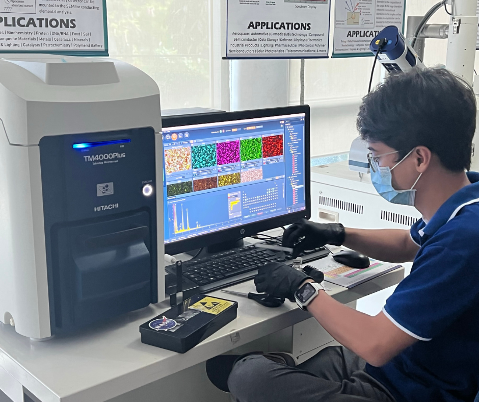
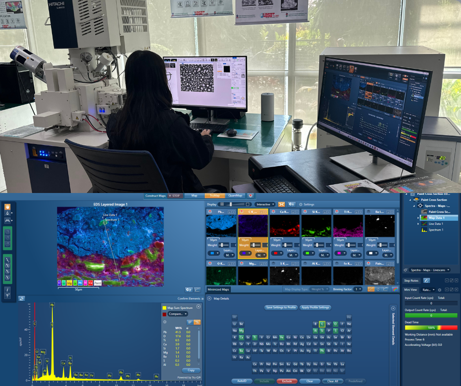
Energy Dispersive X-ray Spectroscopy (EDS or EDX), when integrated with Scanning Electron Microscopy (SEM), enables elemental analysis of materials at the microscale. As the electron beam interacts with the sample, it generates characteristic X-rays that are detected and analyzed to determine the elemental composition of the material.
This technique is widely used for identifying unknown materials, mapping elemental distributions, and supporting failure analysis. It is non-destructive, requires minimal sample preparation, and can detect nearly all elements (except hydrogen and helium). SEM-EDS is applicable to a broad range of materials including metals, ceramics, polymers, and composites.
Common Applications
- Materials Identification
Determines elemental composition of metals, ceramics, polymers, and composites
- Failure Analysis
Investigates fractures, corrosion, and defects in components and assemblies
- Contaminant Detection
Identifies foreign particles or residues in manufacturing and cleanroom environments
- Elemental Mapping
Visualizes spatial distribution of elements across surfaces or cross-sections
- Microelectronics & Semiconductors
Analyzes solder joints, thin films, and interconnects for quality control
- Forensic Science
Examines trace evidence such as gunshot residue, paint chips, and unknown materials
- Geology & Mineralogy
Characterizes mineral phases and inclusions in rock samples
- Coatings & Surface Treatments
Evaluates layer composition, thickness, and uniformity
- And much more.
SEM-EDS is a versatile tool for rapid, localized elemental analysis across research and industry.