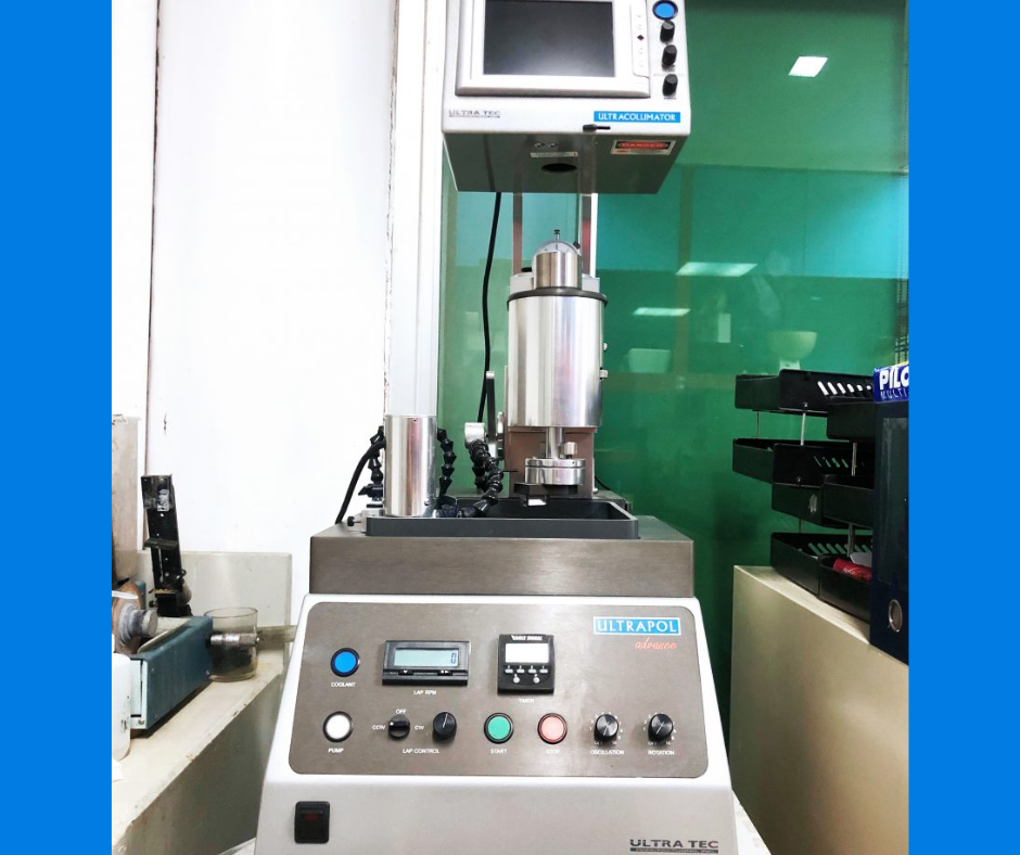
Grinding and polishing are essential sample preparation techniques used to produce flat, smooth surfaces for microscopic and analytical examination. These processes remove surface irregularities, scratches, and deformation layers, enabling accurate imaging and measurement in techniques such as SEM, EBSD, EDS, and optical microscopy.
We offer both manual and automated preparation methods, tailored to the material type and analysis requirements. Proper grinding and polishing improve data quality and reduce artifacts, especially in high-resolution or crystallographic studies.


