Service Details
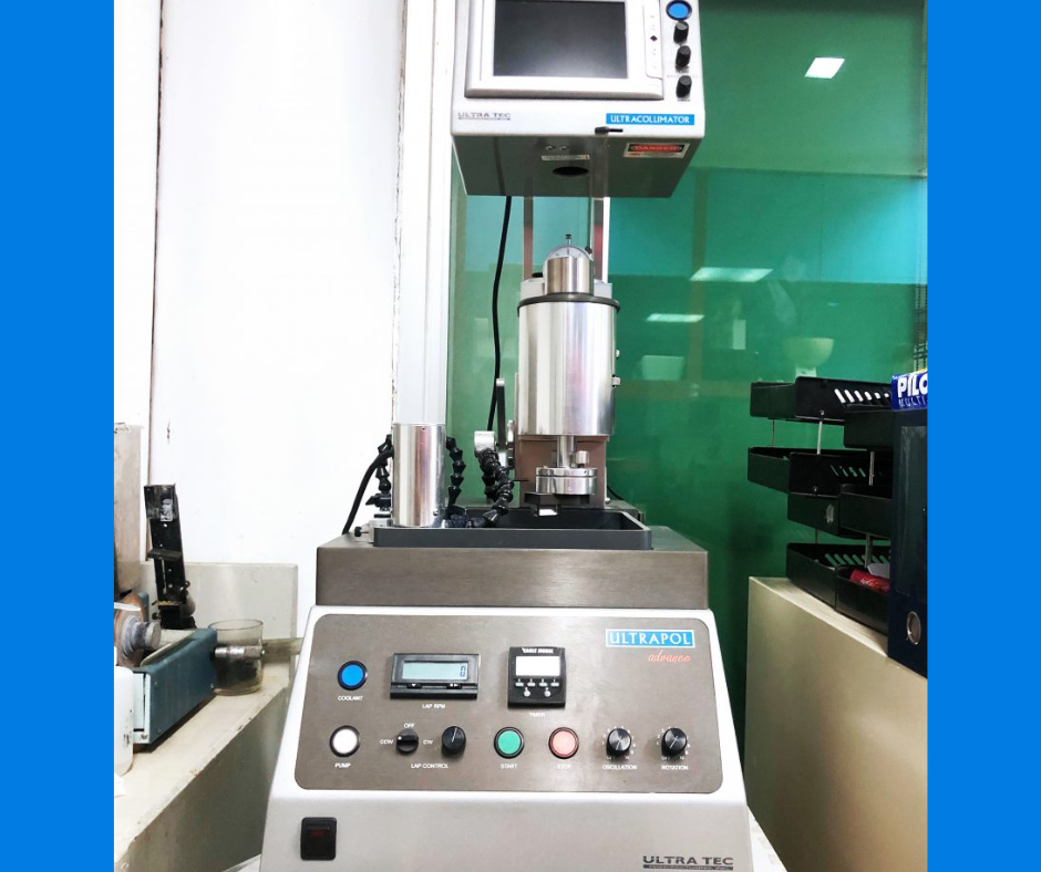
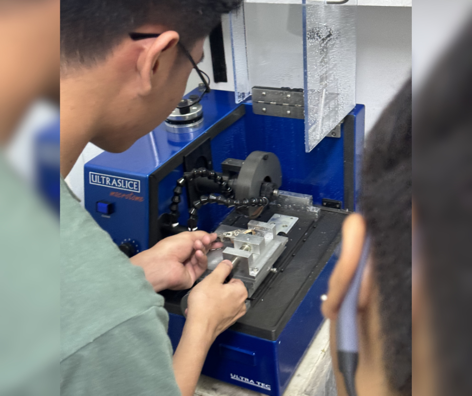
Grinding and Polishing is a sample preparation process used to produce flat, smooth, and properly prepared sample surfaces for microscopic and analytical examination. It helps remove surface irregularities, scratches, and preparation-related damage so the material can be examined more clearly using techniques such as metallography, SEM, EBSD, AFM, and other related microscopy methods.
This process is commonly used in material characterization, failure analysis, cross-section preparation, and research applications. Proper grinding and polishing help prepare representative sample surfaces for more reliable observation of material structures, defects, coatings, interfaces, and other features of interest.
Common Applications
- Metallographic Sample Preparation – Preparation of metal and material samples for microstructure, grain, phase, and defect examination
- SEM Sample Preparation – Producing flat and polished surfaces for high-magnification surface or cross-section imaging
- EBSD Sample Preparation – Preparing smooth, low-damage surfaces for crystallographic orientation and grain structure analysis
- Cross-Section Preparation – Revealing internal layers, interfaces, coatings, packages, and material structures
- Failure Analysis – Preparing samples for investigation of cracks, fractures, corrosion, defects, and material interfaces
- Electronic & Semiconductor Samples – Preparation of die, package-level devices, wafers, and backside surfaces for inspection or further analysis
- Research & Quality Control – Consistent sample preparation for material comparison, product evaluation, and process troubleshooting
- And much more