Service Details
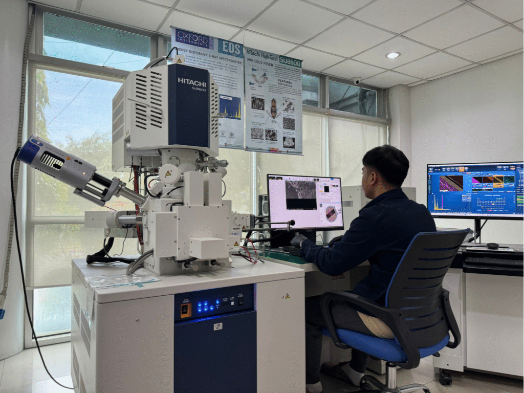
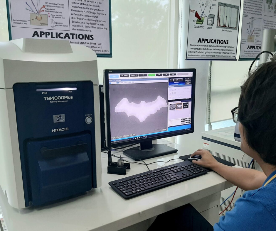
Scanning Electron Microscopy (SEM) imaging is a versatile characterization technique used to analyze a wide variety of samples, including membranes, filters, coins, and even biological specimens such as plant leaves and insects. The Scanning Electron Microscope (SEM) employs electron beams to capture high-resolution images, enabling detailed observation of surface morphology, topography, cracks, failures, and other microscopic features from the micron to the nanoscale level.
To support materials engineering, research, nanotechnology, and failure analysis, NASAT Labs is equipped with five different SEMs, including a cold field emission SEM (FE-SEM) capable of ultra-high resolution imaging down to 0.6 nm. Paired with advanced technologies like EDS and EBSD, our SEM systems deliver cutting-edge performance for surface and elemental analysis. With top-tier instrumentation and regularly trained staff, we ensure precision, reliability, and excellence in every analysis.
Common Applications
-
Materials Science & Engineering
- Surface morphology and microstructure analysis of metals, ceramics, polymers, and composites
- Quality control and failure analysis in manufacturing
- Nanomaterials research (e.g., nanotubes, nanowires, and nanofibers)
-
Semiconductor & Microelectronics
- Inspection of wafers, microchips, and integrated circuits
- Topographical and compositional analysis for fabrication and R&D
- Process control in micro- and nano-lithography
-
Biological & Life Sciences
- Imaging of cells, tissues, bacteria, viruses, and insects
- Structural studies in taxonomy, entomology, and pathology
- Vaccine development and biomedical research
-
Geology & Earth Sciences
- Mineral and soil analysis for morphology and elemental composition
- Weathering studies and petrographic investigations
- Applications in mining and environmental science
-
Forensic Science
- Gunshot residue (GSR) detection and analysis
- Examination of fibers, paint, inks, and tool marks
- Document and counterfeit analysis
-
Medical Research
- Comparative analysis of blood and tissue samples
- Drug efficacy and disease pathology studies
- Development of medical implants and diagnostics
-
Nanotechnology & Surface Science
- Characterization of nanostructures and thin films
- Surface coatings and interface studies
- Micro/nano fabrication and manipulation
-
Art & Digital Imaging
- Creation of high-resolution micrographs for digital art
- Visualization of textures and patterns at the nanoscale
-
And much more