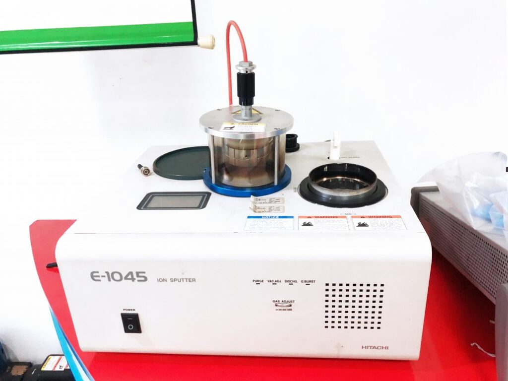
Non-conductive samples often experience a charging effect due to the accumulation of electrons on their surface, which can interfere with obtaining high-quality images. Ion Sputtering coating addresses this issue by allowing imaging at higher beam energies, thereby achieving the highest resolution and magnification without the concern of electron charge effects or beam damage to sensitive samples.
Key Benefits:
- Enhanced Imaging Quality: By mitigating the charging effect, Ion Sputtering enables clearer and more detailed imaging of non-conductive samples.
- Protection of Sensitive Samples: This technique prevents beam damage, ensuring that delicate samples remain intact during analysis.
- Versatility: Ion Sputtering is applicable to a wide range of materials, making it a valuable tool in various fields such as materials science, electronics, and biological research.
Ion Sputtering is an essential preparation step for advanced imaging techniques, ensuring that samples are well-prepared for high-resolution analysis and accurate data collection.