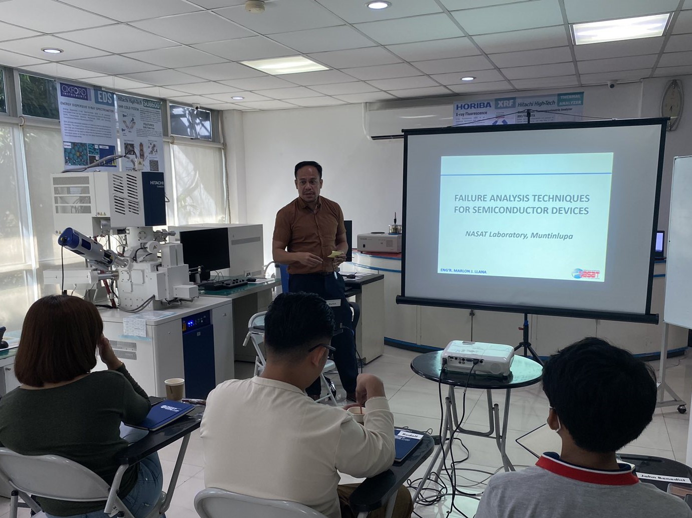
Failure Analysis Techniques for Semiconductor Devices (FA101)

About this Training

This course is a lecture-discussion on the failure analysis techniques in semiconductor devices. This will cover topics from electrical characterization of MOSFET (Igss, Idss, Bvdss etc), non-destructive, destructive analysis up to the application of Photon emission, Optical Beam Induced Resistance Change (OBIRCH), Thermal Emission to failure isolation. Practical tips based on actual experience of the resource speaker will be shared in the training.

Engr. Marlon Llana, M. Sce. Eng.
About the Speaker
Engr. Marlon Llana, M. Sce. Eng.
Technical and Operations Director, NASAT Labs
Eng’r. Llana has a B.S. and a Masters’ degree in Chemical Engineering from Mapua Institute of Technology. He is currently pursuing a doctorate degree in the same institution. He has over 20 years of experience in the semiconductor industry in the field of Quality, R&D, Laboratory Operation, Electro-plating, Failure Analysis and Reliability having worked for Philips Semiconductors, SunPower Mfg. Ltd., International Rectifier, and DECA Technologies. He is also a technical assessor of DTI-PAB for ISO/IEC17025 and is a member of DTI Technical committee for nanotechnology.

Training Schedule

Session 1
JANUARY 18-19
Session 2
AUGUST 6-9
Session 3
NOVEMBER 14-15
  • Customer-site trainings and private webinar trainings are available.
    (Contact us for more information.)